Quick Answer
Visual AI inspection for PCB assembly quality control uses computer vision and machine learning to detect and classify defects such as missing or misaligned components, polarity errors, tombstoning, solder bridges, lifted components, and other visible assembly abnormalities. It can complement traditional AOI by learning production variations, helping reduce false calls, improving defect classification, and connecting inspection results with broader manufacturing quality data. Visual AI can also correlate inspection stages such as SPI and AOI to support root-cause analysis, while X-ray, ICT, and functional testing remain important for defects that optical inspection cannot see.
Printed circuit board assembly is becoming increasingly difficult to inspect consistently. Components are getting smaller, boards are becoming denser, production lines are handling more product variants, and manufacturers are expected to maintain quality without slowing throughput.
Automated Optical Inspection (AOI) has long been central to PCB assembly quality control. However, conventional AOI systems typically depend on predefined measurements, thresholds, templates, and inspection rules. Normal manufacturing variation can therefore produce false calls that send good boards for unnecessary manual inspection. Research based on 132 days of real-world SMT production data specifically identifies false calls as a source of significant manual inspection effort.
This is where visual AI inspection for PCB assembly quality control can add value.
Visual AI uses computer vision and machine learning to analyze PCB images, distinguish acceptable manufacturing variation from potential defects, classify abnormalities, and provide quality teams with more contextual inspection information.
The objective is not necessarily to replace AOI. Instead, manufacturers can use AI to make existing inspection workflows more intelligent, adaptive, and connected to the broader quality process.
What Is Visual AI Inspection for PCB Assembly Quality Control?
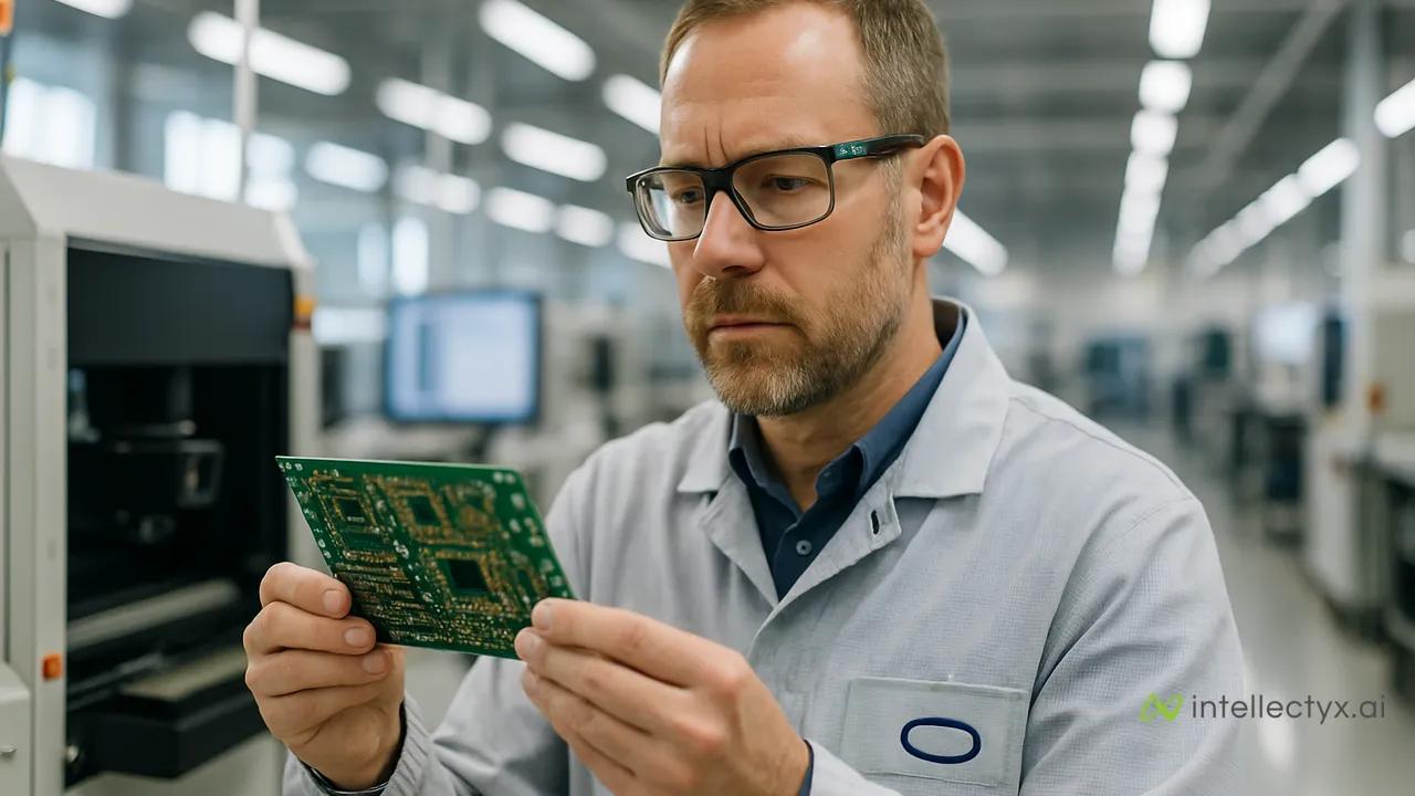
Visual AI inspection for PCB assembly quality control uses computer vision and machine learning to analyze PCB images and identify assembly defects such as missing components, misalignment, incorrect orientation, polarity errors, tombstoning, solder bridges, insufficient solder, lifted leads, contamination, and surface abnormalities.
A simplified workflow looks like this:
PCB → Image Capture → AI Analysis → Defect Detection → Defect Classification → Pass / Review → Quality Record
Traditional AOI generally measures visual characteristics against predefined rules or limits. AI-based inspection introduces models capable of learning patterns from production data and using those patterns to classify inspection results.
A large review of automatic PCB inspection research notes that AI approaches have increasingly been introduced to improve visual inspection performance and reduce operating costs.
Visual AI can be applied at different stages of PCB assembly, but its role should depend on the defect being inspected.
Why Is PCB Assembly Quality Control Becoming More Difficult?
PCB quality control is no longer simply about identifying whether a component is present.
Modern electronics manufacturing involves:
- High-density PCB assemblies
- Miniaturized components
- Fine-pitch devices
- Complex component orientation
- High-speed SMT production
- Frequent product changeovers
- Multiple PCB variants
- Strict reliability requirements
- Increasing amounts of inspection data
A single PCB can contain hundreds or thousands of inspection points.
The challenge becomes even greater in high-mix manufacturing, where the same production environment handles many different board configurations.
Rule-based inspection systems need appropriate parameters for these variations. When thresholds are overly sensitive, acceptable boards may be flagged for review. When they are too permissive, defects risk escaping downstream.
Visual AI provides another layer for evaluating these variations.
How Does Visual AI Inspect PCB Assemblies?
Visual AI inspection typically combines industrial cameras, controlled lighting, image-processing pipelines, computer vision models, and manufacturing integration.
Step 1: Capture the PCB Image
High-resolution cameras capture images of the assembled board.
The inspection environment needs consistent:
- Lighting
- Camera positioning
- Focus
- Resolution
- Viewing angle
Image quality matters because AI cannot reliably analyze visual information that the camera itself cannot capture.
Step 2: Locate Components and Inspection Regions
The vision system identifies relevant areas of the board, such as components, pads, solder joints, connectors, markings, or other regions of interest.
Step 3: Analyze Visual Characteristics
AI models compare what they see with patterns learned during training.
Depending on the system, models may perform:
- Object detection
- Image classification
- Segmentation
- Anomaly detection
- Optical character recognition
Step 4: Identify Potential Defects
The model determines whether the observed condition resembles an acceptable assembly or a potential defect.
Step 5: Classify the Defect
Instead of simply returning "fail," the system can potentially categorize the issue.
For example:
Missing Component → Polarity Error → Misalignment → Solder Bridge → Surface Defect
Step 6: Route the Result
High-confidence acceptable boards can continue through the appropriate production process.
Potential defects or low-confidence cases can be sent for human review.
Step 7: Store Inspection Data
Results can be connected with MES, QMS, traceability, or product-genealogy systems for further quality analysis.
The result is not just automated inspection. It creates structured visual quality data that can potentially be used for broader manufacturing intelligence.
What PCB Assembly Defects Can Visual AI Detect?
The exact defects depend on camera visibility, lighting, training data, board design, component type, and inspection architecture.
However, common visual inspection applications include the following.
Component Placement Defects
Visual AI can help identify:
- Missing components
- Incorrect components
- Misaligned components
- Incorrect orientation
- Polarity errors
- Tombstoning
- Lifted components
- Placement abnormalities
Visible Solder Defects
Depending on image quality and inspection configuration, AI can assist with identifying:
- Solder bridges
- Insufficient visible solder
- Excess solder
- Abnormal solder-joint appearance
- Visible soldering inconsistencies
Surface and Assembly Defects
AI inspection can also support detection of:
- Scratches
- Contamination
- Foreign material
- Surface abnormalities
- Connector issues
- Label problems
- Coating abnormalities
Current vision-AI platforms for PCB assembly describe applications spanning solder paste, pre- and post-reflow inspection, components, conformal coating, markings, and final quality control.
However, there is an important limitation.
If a defect cannot be seen by the camera, ordinary visual AI cannot magically detect it from an external image.
Hidden solder joints, internal electrical faults, intermittent behavior, and certain package-related defects may require X-ray inspection, in-circuit testing, functional testing, or other methods.
How Can Visual AI Reduce False Calls in PCB Inspection?
False calls occur when an inspection system identifies an acceptable board or component as defective.
Consider a PCB with an acceptable solder joint whose visual appearance differs slightly because of lighting, material variation, or production conditions.
A rigid threshold could interpret that difference as a defect.
The workflow becomes:
Good PCB → AOI Alert → Manual Inspection → Operator Confirms Good → PCB Returned to Production
Repeat this across thousands of inspection points and manual review becomes an operational bottleneck.
AI can provide an additional decision layer:
AOI Alert → AI Analysis → Likely True Defect / Likely False Call / Uncertain → Human Review Where Needed
The purpose should not be to loosen quality requirements.
It should be to better distinguish actual defects from acceptable manufacturing variation.
How Can AI Connect SPI and AOI for Better PCB Quality?
This is one of the more interesting developments in AI-based electronics quality control.
PCB inspection stations have traditionally generated useful information but often operate independently.
Consider the SMT workflow:
Solder Paste Printing → SPI → Pick & Place → Reflow → AOI
A post-reflow defect may actually originate much earlier in the process.
For example:
Abnormal Solder Paste → Component Placement → Reflow → Solder Defect Detected by AOI
If SPI and AOI data are analyzed separately, quality engineers see two individual inspection events.
AI can help correlate them.
That changes the question from:
"Which board failed?"
to:
"What process condition may have caused this board to fail?"
This is an important evolution from automated inspection toward manufacturing quality intelligence.
How Is Visual AI Being Used in Electronics Manufacturing?
The usefulness of AI in electronics and hardware engineering extends beyond PCB defect detection.
Electronic Component Inspection
Computer vision can inspect components for visual abnormalities, markings, orientation, surface condition, and other visible characteristics.
PCB Assembly Inspection
AI can identify placement, soldering, polarity, and assembly abnormalities.
Process Monitoring
AI models can identify unusual production patterns that may indicate emerging quality problems.
Defect Classification
Instead of presenting operators with generic inspection failures, AI can categorize defects and help prioritize investigation.
Root-Cause Investigation
Inspection information can be combined with process, equipment, supplier, and production data to help engineers investigate recurring defects.
Predictive Quality
Historical quality patterns can potentially be used to identify manufacturing conditions associated with higher defect risk.
AI therefore has practical applications in electronics manufacturing, but the strongest use cases tend to be specific operational problems, not generic "AI for engineering."
What Is the Role of AI Robotics in PCB Manufacturing?
AI robotics in PCB manufacturing combines machine vision with automated equipment to improve handling, inspection, sorting, assembly verification, and other production tasks.
A typical workflow might be:
Robot Handles PCB → Camera Captures Board → AI Inspects Assembly → Quality Decision → Robot Routes Board
For example, boards identified as acceptable could continue to the next stage, while potential defects are routed to inspection or rework.
AI vision can also support robotic systems by helping them understand differences between products rather than depending exclusively on fixed coordinates and predefined conditions.
Potential applications include:
- PCB handling
- Automated inspection
- Defect sorting
- Assembly verification
- Material movement
- Rework assistance
However, AI robotics should be deployed where it solves a measurable production constraint rather than adding automation simply because the technology is available.
How Are AI Modules Used in PCB Assembly?
The phrase AI module PCB assembly can describe two different scenarios.
First, an AI module may form part of the inspection infrastructure.
Edge-computing devices can run computer vision models close to the production line so image analysis does not always need to be sent to a remote cloud environment.
A possible architecture is:
Industrial Camera → Edge AI Module → Vision Model → Inspection Decision → MES/QMS
This can support real-time inspection while keeping production data close to the manufacturing environment.
Second, PCB manufacturers increasingly assemble products containing processors, NPUs, GPUs, sensors, and other hardware designed for AI-enabled products.
These boards may involve high-density designs and advanced packaging that require sophisticated inspection strategies.
The important point is that AI can exist both inside the product and inside the manufacturing process used to inspect that product.
Where Should Visual AI Be Deployed on an SMT Line?
There is no single best inspection point.
Different defects become visible at different stages.
1. Solder Paste Inspection
SPI evaluates solder paste before component placement and can identify printing abnormalities early.
2. Pre-Reflow Inspection
Vision systems can check whether components have been placed correctly before the board enters reflow.
3. Post-Reflow AOI
This is a major inspection stage for identifying visible placement and soldering defects after reflow.
4. Automated X-Ray Inspection
AXI is important where solder joints or structural characteristics are hidden from ordinary optical cameras.
5. Final Visual Inspection
Visual AI can inspect connectors, labels, surfaces, coatings, and other final assembly characteristics.
6. Electrical and Functional Testing
Visual inspection cannot determine whether every electrical circuit or function performs correctly.
ICT, flying probe, functional testing, and other electrical verification techniques therefore remain important.
The strongest PCB quality strategy uses the appropriate inspection technology for the appropriate failure mode.
How Does Visual AI Improve PCB Assembly Quality Control?
Visual AI can create value in several areas.
Earlier Defect Detection
Finding defects earlier prevents them from progressing into downstream assembly, testing, or shipment.
More Consistent Inspection
AI can apply the same learned inspection logic repeatedly rather than depending entirely on subjective manual inspection.
Reduced Manual Reinspection
Better classification of inspection results can help quality teams focus their attention on genuine or uncertain defects.
Better Handling of Product Variation
AI models can learn patterns of acceptable production variation that are difficult to capture with simple fixed thresholds.
Faster Quality Feedback
Inspection results can be fed back into manufacturing processes faster.
Better Defect Traceability
Visual inspection results can be associated with board serial numbers, production conditions, and other manufacturing records.
Improved Root-Cause Investigation
When inspection information is connected with production data, AI can help engineers investigate why recurring defects occur.
Expert Perspective
“AI has shown significant potential in the realm of AOI.”
Matt Kelly, CTO and VP of Technology Solutions, IPC
How Can Visual AI Support PCB Root-Cause Analysis?
Defect detection answers:
What went wrong?
Manufacturing intelligence needs to answer:
Why did it go wrong?
Suppose post-reflow visual inspection detects an unusual increase in solder bridges.
Instead of reviewing each defect individually, an AI-enabled workflow could investigate:
Defect Detected
↓
Retrieve PCB Serial Number
↓
Retrieve SPI Measurements
↓
Check Production Line
↓
Analyze Reflow Parameters
↓
Check Material/Component Lot
↓
Compare Similar Failures
↓
Surface Potential Root Causes
This is where connecting visual AI with MES, QMS, equipment, and traceability information becomes valuable.
The inspection image becomes one part of a larger quality record rather than an isolated pass/fail decision.
Fraunhofer IZM's work on connecting SPI and AOI through AI demonstrates this direction toward inspection systems that help explain defects across manufacturing processes.
How Can Visual AI Support Electronics Recall Prevention?
A defect caught on the production line is generally easier to manage than one discovered after thousands of products have shipped.
Visual AI can contribute to recall prevention by identifying assembly abnormalities earlier and creating better traceability around inspection outcomes.
The progression can look like:
Visual Defect → PCB Serial Number → Component/Process Investigation → Potentially Affected Production → Containment
If inspection results are connected with component genealogy, manufacturers can also investigate whether similar boards contain the same component lot or share the same production conditions.
This connects PCB inspection with a broader AI-driven recall management strategy.
Instead of treating quality inspection, traceability, root-cause analysis, and recall readiness as separate activities, manufacturers can connect them through shared production intelligence.
How to Implement Visual AI Inspection for PCB Assembly
A successful implementation should begin with the manufacturing problem, not the AI model.
Step 1: Define the Quality Problem
Identify what needs improvement.
Examples include:
- Excessive AOI false calls
- Recurring solder defects
- Missed component errors
- High manual inspection workload
- Slow product changeovers
- Quality escapes
- Difficult root-cause investigations
Step 2: Choose the Inspection Point
Determine where the defect is visible and where intervention creates the most value.
Step 3: Collect Representative Production Data
Training and validation data should represent real production conditions, including:
- Good boards
- Confirmed defects
- Product variants
- Different component lots
- Acceptable manufacturing variation
- Relevant lighting and imaging conditions
Step 4: Train and Validate the Vision Model
Evaluate the model using actual production data.
Important metrics include:
- True defect detection
- False positives
- False negatives
- Confidence
- Processing time
Do not evaluate accuracy alone. A system that detects defects but overwhelms operators with false alerts may still create a poor production outcome.
Step 5: Integrate with Existing Inspection Systems
Manufacturers do not necessarily need to replace AOI infrastructure.
AI can be introduced as an additional classification or intelligence layer.
Step 6: Connect Manufacturing Systems
Where useful, integrate inspection results with:
MES + QMS + Traceability + Product Genealogy + Process Data
This enables broader quality analytics and root-cause investigation.
Step 7: Keep Humans in the Review Loop
Low-confidence and unusual conditions should be routed to qualified inspectors or engineers.
Their confirmed decisions can also become valuable feedback for improving the model.
Step 8: Monitor Models in Production
Manufacturing conditions change.
New PCB variants, components, materials, suppliers, equipment settings, and production conditions can alter visual patterns.
AI models therefore require continuous monitoring and appropriate retraining.
Why Choose Intellectyx for Visual AI Inspection in Electronics Manufacturing?
Electronics manufacturers typically do not need another standalone AI demonstration. They need AI that can operate within existing production and quality environments.
Intellectyx helps electronics and manufacturing enterprises build custom AI solutions that connect computer vision, manufacturing intelligence, AI agents, and operational workflows.
Relevant capabilities include:
Visual AI Solutions
Build custom computer vision models for PCB, component, assembly, and manufacturing quality inspection.
Custom AI Agents
Quality agents can retrieve inspection history, manufacturing records, component information, test results, and related evidence to support defect investigations.
Agentic AI Strategy
Move beyond isolated defect detection toward workflows where AI can investigate quality problems, gather context, recommend actions, and escalate decisions.
Enterprise AI Solutions
Integrate AI with existing MES, QMS, traceability, and manufacturing environments instead of creating another disconnected quality application.
AgentOps
Monitor AI models and agents operating in production, including performance, confidence, failures, exceptions, and human overrides.
The objective is not necessarily to replace an electronics manufacturer's existing AOI equipment.
It is to add intelligence across inspection and quality workflows so manufacturers can move from detecting defects toward understanding and preventing them.
Final Thoughts
Visual AI inspection for PCB assembly quality control represents an evolution of electronics quality management rather than a simple replacement for existing inspection equipment.
Traditional AOI remains highly effective for repeatable optical inspection. SPI remains important for solder-paste quality. AXI can inspect characteristics hidden from optical cameras. ICT and functional testing verify electrical and functional behavior.
Visual AI adds another capability:
the ability to learn from manufacturing data and help interpret what inspection systems are seeing.
That can help electronics manufacturers reduce unnecessary manual review, improve defect classification, connect inspection stages, and investigate quality problems more effectively.
The larger opportunity emerges when visual AI becomes connected with manufacturing data.
Inspection → Classification → Traceability → Root-Cause Analysis → Process Improvement → Recall Prevention
That is where PCB inspection begins to move beyond pass/fail automation and toward intelligent, connected quality control.